Guide to Reballing for Different BGA Package Types
Reballing, or reworking, is a crucial process for repairing poorly connected ball grid array packages. Given the various BGA package sizes and types, solder types and reworking techniques can differ. Understanding the basics will help you decide where to send your BGA packages for reballing.
Table of Contents
- What Is a Ball Grid Array Package?
- Advantages of BGA Packages
- BGA Package Types
- Additional BGA Package Types
- Connect With Us for All Your BGA Rework, Training and Consulting Needs
What Is a Ball Grid Array Package?
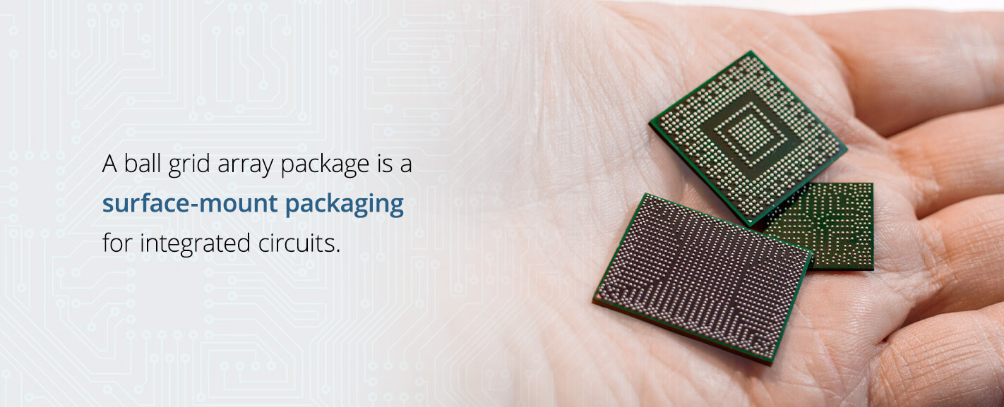
A ball grid array package is a surface-mount packaging for integrated circuits. This component does not have leads connecting it to a circuit board. Instead, it uses solder balls to create electrical connections between the circuit board and the package. These attach to the substrate, which is wire-bonded to the die. Conductive traces within the substrate facilitate electrical signals from the die to the solder balls.
Reballing BGA packages allows you to reuse components instead of scrapping them. This process saves money and materials by removing and reconnecting the BGA package. Reworking BGA packages can reduce repair costs by up to 25% compared to quad flat-pack packages.
Advantages of BGA Packages
Using solder to affix the BGA package to the substrate is beneficial for many reasons.
- Compact size: These packages take up less space on the circuit board.
- Self-alignment: The solder joints' spherical shape aids in easy alignment.
- Thermal performance: Heat quickly dissipates between the joints, reducing thermal resistance.
- High conductivity: Numerous small-sized solder joints allow for better electrical movement through the balls of the package.
BGA Package Types
BGA packages come in various kinds and sizes, each defined by the materials used in their substrates. The primary BGA package types include ceramic, plastic laminate and tape.
The solder composition matters when reballing these BGA package types. Each requires specific solder compositions to ensure optimal conductivity and durability during reworking.
1. Ceramic BGA
The ceramic ball grid array package uses a ceramic substrate. Subtypes within this category include ceramic column grid array and land grid array packages.
CBGA packages are generally more expensive per pin. However, some applications require this type, such as devices that require a high pin count on flip-chip designs. Other materials cannot achieve the density needed for those uses.
CBGA packages also work well with flip chips in general. The solder balls typically comprise 90% lead and 10% tin, enhancing reliability by addressing thermal expansion differences between the substrate and the board.
However, you may also find ceramic column grid array packages. With their columnar solder joints, these packages offer nearly double the contact points and triple the life span of standard BGAs.
2. Plastic Laminate
Plastic BGA packages use a plastic substrate and solder balls composed of 63% tin and 37% eutectic lead. The substrate materials must withstand temperatures up to 302 degrees Fahrenheit, with common choices including the following.
- Dry-clad: IBM's proprietary epoxy-based laminate.
- Polyimides: A form of plastic laminate.
- BT epoxy glass: Bismaleimide triazine epoxy glass.
PBGA can also accommodate flip-chip designs to increase connectivity between the package and the circuit board.
3. Tape
TBGA packages use flexible interconnects to create fine lines on the solder balls. This configuration excels at thermal performance.
Similarly, metal BGA uses an aluminum substrate in the simplest design form. While it does not use tape or a flex layer like TBGA packages, its design produces similar results. It harnesses thin film and microchip module technology to connect the solder mask to the aluminum base. Metal and tape have similarly outstanding electrical and thermal performance.
Additional BGA Package Types
There are four additional types to consider besides the three primary BGA packages.
1. Package-on-Package
Package-on-package designs feature a double-stack configuration. The top chip is for random access memory, while the bottom chip is the central processing unit. This design allows more packages to fit into a smaller footprint on the circuit board, optimizing space.
2. Land Grid Array
Land grid array packages were precursors to BGA packages. This design introduced the need for BGA package types in the 1990s by requiring solder balls to connect the package to the circuit board. For LGAs that use sockets, the package includes pins to connect the socket to the circuit board.
Other LGAs connect directly to the circuit board through soldering rather than a socket. Unlike BGA package types, LGA packages have flat solder contacts instead of balls.
3. Quad Flat No-Lead
Quad flat no-lead packages are surface-mounted chips that send leads from all four sides. This package type's use of all four sides gives it the “quad" part of its name. They come with plastic and ceramic substrates. Plastic QFP types all have gull-wing leads, whereas ceramic QFP does not.
There is also a quad flat pack with no leads or pins, abbreviated QFN.
4. Flip-Chip
The flip-chip ball grid array package places the active site downward. Any surface of a flip-chip can have connections through solder ball joints. Using a flip-chip BGA reduces distance and inductance.
Connect With Precision PCB Services for All Your BGA Package Needs
If you need reworking on a part, you get a wholly revived system, not just a machine. For over 25 years, Precision PCB Services has been a reliable partner for BGA, QFN and CGA reballing services. We also offer comprehensive training and consulting services.
Contact us online today for expert assistance.